Our lab is all about exciting experiments with powerful ultrafast laser light and electron beams in electron microscopes, with an eye towards practical, applied physics.
While the lab is de-facto under construction, there is just so much to do in the meantime.. Join us!
Background
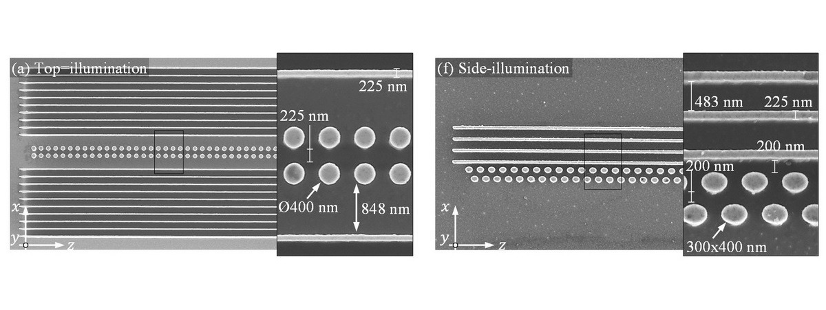
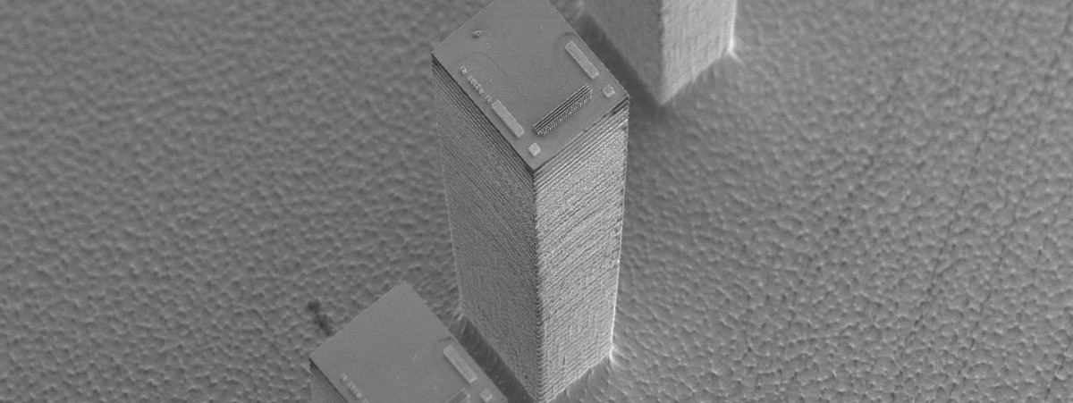
The concept of dielectric laser acceleration (DLA) can be traced back to the 1960s, shortly after the invention of the laser. At the time, laser and fabrication technology were not mature enough to compete with radio-frequency (RF) acceleration, which nowadays is the power-horse behind the large accelerator facilities. The main trade-off between the two technologies lies in the average electron current and average acceleration gradient: RF acceleration traditionally uses metallic cavities and RF fields, and is thus limited by the electrical breakdown of the cavities at acceleration gradients of roughly 25-50 MeV/m. Hence, an energy gain of e.g. 50 MeV by an electron requires ~1 meter. The breakdown field of dielectric materials can reach even 9 GV/m, and an average acceleration gradient in DLA of 850 MeV/m and 1.8 GV/m accelerating fields have already been shown. With DLA technology, 50 MeV can potentially be imparted within down to about 1 cm or less. Importantly, the orders of magnitude higher acceleration gradient implies orders of magnitude smaller devices: indeed, various demonstrations of electron acceleration on a chip are, today, widely recognized, both in the sub-relativistic and relativistic regimes. Interestingly, classical treatment of DLA still offers rich and complex electron beam dynamics, including attosecond train generation and various demonstrations of beam control. The nanostructures employed today are generally of the so called “dual pillar” type, however, photonic inverse design techniques have already been introduced and are expected to produce more efficient and versatile electron-manipulating nanophotonic designs.
Nanophotonic laser accelerator research is unique in its versatile ability to produce electron beams with sufficient quality for high-resolution electron microscopy at nearly-arbitrarily-high electron energies, and pulses at MHz repetition rates which are only limited by the laser technology. Nanophotonic accelerators are at the interface between matter waves, photons, classical electromagnetics, nanofabrication, and quantum science. From there, they extend long arms that potentially reach the realm of high-energy particle physics, material science, quantum electrodynamics, and at the same time real-world applications such as miniature medical irradiation devices.
In the news
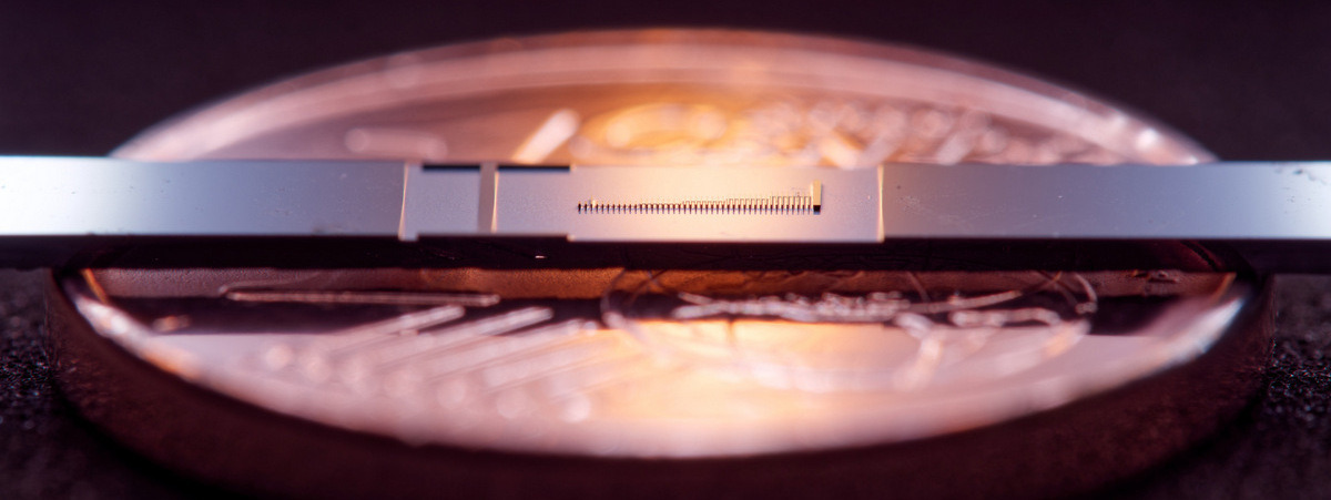
 Our latest nanophotonic electron on-chip accelerator Nature publication was recently covered in Haaretz, along with a huge splash in other news outlets and mainstream media in the world. Here are some of them:
-
The compact accelerator that keeps electrons on the straight and narrow – Yelong Wei in nature News and Views
-
Tiniest particle accelerator is so small it could fit into a pen tip – Karmela Padavic-Callaghan in New Scientist
-
Tiny accelerators get electrons up to speed using lasers – Emily Conover in ScienceNews
-
Particle Accelerator on a Chip Hits Penny-Size – Charles Q. Choi in IEEE Spectrum
-
Electrons accelerated by firing lasers into nanophotonic cavities – Tim Wogan in Physicsworld
-
Milestone: Miniature particle accelerator works – Blandina Mangelkramer in Research-in-Germany
-
Milestone: Miniature particle accelerator works – ScienceDaily
-
Solar Surprise: The Sun’s magnetic poles will flip earlier than expected – Sabine Hossenfelder on Youtube
- How physicists built the world’s smallest particle accelerator – Rahul Rao in Popular Science
- Revolutionary Chip-Sized Particle Accelerator Promises a New Era in Medical Treatment – Govind Tekale in KarmaActive
-
Coherent electron acceleration using photonic nanostructures – published in Nature – published at the FAU "Lehrstuhl für Laserphysik" in Germany, where the experiment was done.
- – Make sure you check out this Instagram reel by Cleoabram!
..Sounds interesting?
Take a journey into Science with us.. Click here for more!!
Open positions
We are currently searching for students interested in theory and simulation of nanophotonics, electron optics, accelerator physics, and quantum electron-photon interactions. Join us and be exposed to and engage in diverse, research-front topics:
- Particle accelerators
- Electron optics
- Nanophotonics
- Nanofabrication
- Light-matter interaction at the quantum limit
This includes Bachelor students looking to work on their final project, MSc and PhD applicants, and possibly also per-hour mini-jobs. International applicants, post-docs, are also encouraged to apply!
More details are just an email away!
|
Roy Shiloh, roy.shiloh@mail.huji.ac.il |


